This page discusses the losses in a typical boost converter which can be used to calculate the efficiency of the Boost regulator working in Continuous conduction mode.
Definition
Efficiency ($η$) in general is defined as:Since Input power is the sum of Output power and all the power lost we have:
So we just need to calculate all the power losses in the circuit and we can then calculate the efficiency of the circuit.
The circuit
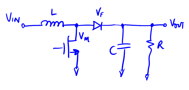
The Boost circuit can be drawn as:
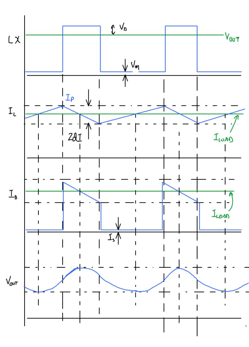
The circuit waveforms look like:

The circuit working is well known and is explained as follows. When MOS power switch turns ON then the inductor sees a nearly constant DC voltage (
$V_{in+$) across it and so the current in the inductor ramps up linearly. When the MOS power switch turns OFF then since the current in the inductor cannot go to 0 instantaneously, it charges up the drain node of the Power FET (the parasitic cap) and keeps charging it until it cap voltage reaches a diode voltage higher than whatever output voltage on $V_{out}$ exists. At this time the diode turns ON and the inductor current starts charging the output capacitor. For the inductor current to actually decrease the $V_{out}$ plus a diode voltage should be more than $V_{in}$ so that the inductor sees a DC voltage of $V_{out}+V_d-V_{in}$ across it with the drain of the power FET being positive. This causes the inductor current to ramp down linearly.Now by controlling the ON time and OFF time of the power switch we can control the average current in the inductor and hence create a boost converter which may regulate the average input current, or the output voltage. For calculating efficiency it does not matter what is being regulated all that we need to know is the
$T_{on}$ and $T_{off}$ of the power switch. So now lets start calculating the losses in this circuit.NOTE: The circuit shows a diode, but there may as well be a shottky or a synchronous FET device to transfer the inductor energy to the output capacitor.
The Losses
The losses can be divided into 2 types for the circuit- DC Losses: These losses are the power dissipated in the circuit elements when the current is flowing through them
- AC Losses: These losses are the power losses when the current is being switched
DC Losses
Diode Loss
The diode loss is given as:where
$V_D=V_T\ln[I_D/I_S+1]$ and $I_D=I_P-2dIt/T_{off}$$V_T$ is the thermal voltage$I_D$ is the diode current$I_S$ is the diode reverse saturation current$I_P$ is the Inductor peak current$2dI$ is the inductor current ripple$T$ is the switching period$T_{off}$ is the off time of the switchwe can plug these 2 into the equation and evaluate it to get:
This can be simplified to a simple form which can also be derived assuming that the voltage across the diode does not change significantly and can be taken out of the integral. We then have:
where
$D=T_{ON}/T$ is the Duty cycle of the switching node. MOS and resistor Losses
The combined loss of MOS ON resistance and a current sense resistor if present in series with the MOS device can be calculated by taking the combined resistance of the MOS and the resistor as$R_{SW}$. The power dissipated in this resistor during the MOS ON time is given as:where
$I_M=I_P-2dI+2dIt/T_{on}$ which is the equation to calculate the instantaneous current through the MOS device in the ON cycleThis can be substituted in the integral and solved to give:
Inductor resistance Loss
Let the inductor resistance be$R_L$. The power dissipated in the inductor resistor is given by:where
$I_{LR}=I_P-2dI+2dIt/T_{on}$ is the equation of the inductor current when it is rising$I_{LF}=I_P-2dIt/T_{off}$ is the equation of the inductor current when it is fallingThis can be solved to give the expression:
Thus the term multiplying by
$R_L$ is also the Inductor RMS currentAC Losses
Drain capacitance loss
When the MOS is OFF then the DRAIN capacitance charges to$V_{DRAIN}=V_{OUT}+V_D$. When the MOS switches ON that charge is drischarged to ground and lost. Therefore the capacitor energy lost
$=1/2C_{DRAIN}V_{DRAIN}^2$And capacitor power lost
$=1/2{C_{DRAIN}V_{DRAIN}^2}/T$MOS switching loss
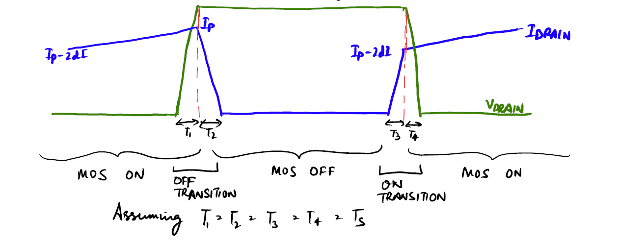
These losses happen as a result of the dissipation in the MOS device when it is not completely OFF and the drain voltage is significant. At this time the MOS device may have lot of current flowing through it with a drain voltage on it thus dissipating a lot of energy. This loss is significant and most of the time cannot be ignored. Let us consider the worst case drain current and voltage of the MOS as shown below:
Let us calculate the losses in the OFF and ON transitions separately:
OFF Transition:
Here
$V_{DR}=V_{DRAIN}t/T_S$ and $I_D=I_P-I_Pt/T_S$Putting these in the integral and solving we have:
ON Transition:
Here
$V_{DR}=V_{DRAIN}(1-t/T_S)$ and $I_M=(I_P-2dI)t/T_S$Putting these in the integral and solving we have:
Combining the OFF and ON transient power losses we have:
Total Power Loss
$=2V_{DRAIN}T_S/T(I_P-dI)$Total Power Loss
So the total Power loss can be written as:where
$D=T_{ON}/T$ is the Duty cycle of the switching node LX$V_D=V_T\ln[I_D/I_S+1]$ is the diode voltage for current $I_D$ which we can take on the average to the load current$I_P$ is the Inductor peak current$2dI$ is the inductor current ripple$R_{SW}$ is the MOS and inductor and any current sense resistor resistance$V_{DRAIN}=V_{OUT}+V_D$ is the output voltage plus the diode voltage$C_{DRAIN}$ is the capacitance on the switching node LX$T_S$ is the voltage/current transition time between ON and OFF$T$ is the switching periodSee Also
- Boost Converter Switching transfer function for stability Analysis
- LX Ringing on Switching Regulators