On This Page
Introduction
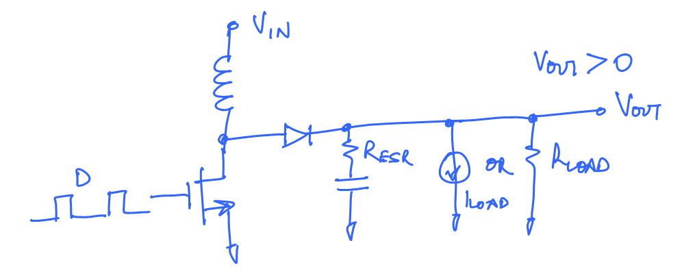
Here we will derive the Boost switching stage transfer function. This can be used to calculate the loop gain expression for a boost converter. Deriving the transfer function is not as intuitive since the control signal is transferred from simple analog signals to a time domain duty cycle signal. The analysis below works on first principles and gets to the final transfer function without applying equivalence of the switching stage to any simplified circuit or transformer. The technique has been very useful to me since the concepts used in this technique are so basic I have been able to analyze all switching regulator architectures using this method.The Circuit

The input to this circuit is the duty cylce D and output is
$V_{out}$. We will derive the large signal and small signal equations relating these 2. The small signal transfer equation can then be combined with the feedback scheme used for the converter to write the full loop gain for the Boost converter. Have the loop gain expression makes it possible to improve stability or enhance the bandwidth of the converter in a systematic way.Large Signal Transfer Function
Consider 2 cycles of switching where the second cycle is slightly different than the first, i.e. a transient change is happening in the loop. The inductor current and values look like:
Setting the following:
Note that:
Similarly:
Average Diode current rate of change
Rate of change of average diode current:$I_D(t+T)-I_D(t) = 1/2(I_4+I_5-I_2-I_3)(1-d)-1/2(I_4+I_5+I_2+I_3){Δd}/2$...(1)Where
$I_2$,$I_3$,$I_4$,$I_5$ can be written as:$I_2={V_{IN}}/L(d-{Δd}/2)T+I_1$ ...(2)$I_3=I_2-(V_{OUT}-V_{IN})/L(1-d+{Δd}/2)T⋍I_1+{V_{IN}}/LT-T/L((V_O-{ΔV_O}/2)(1-d)+V_O{Δd}/2)$ ...(3)$I_4=I_3+{V_{IN}}/L(d+{Δd}/2)T⋍I_1+{V_{IN}}/LT-T/L((V_O-{ΔV_O}/2)(1-d)+V_O{Δd}/2)+{V_{IN}}/L(d+{Δd}/2)T$ ...(4)$I_5=I_4-{V_{OUT}(t+T)-V_{IN}}/L(1-d-{Δd}/2)T⋍I_1+2{V_{IN}}/LT-2T/LV_O(1-d)$ ...(5)Now we can calculate
$ΔI_D=I_D(t+T)-I_D(t)$ by substituting $I_2$,$I_3$,$I_4$ and $I_5$ in (1)Neglecting the
$ΔV_oΔd$ terms and dividing by T we have:${ΔI_D}/T=1/2(2{V_{IN}}/L+{V_{IN}}/LΔd-2V_o/L(1-d))(1-d)-(I_1{Δd}/T+{V_{IN}}/LΔd+{V_{IN}}/Ld{Δd}/2-{V_o}/LΔd(1-d))$.......(6)For the average stability analysis we can easily assume that T is much smaller than the time periods we are interested in. So
$T→0$ and we have the following:${Lt}↙{T→0}D(t+T)=D(t)$, ${Lt}↙{T→0}(1-d)={Lt}↙{T→0}(1-{D(t)+D(t+T)}/2)=1-D(t)$,${Lt}↙{T→0}{Δd}/T={dD(t)}/{dt}$, ${Lt}↙{T→0}Δd={Lt}↙{T→0}D(t+T)-D(t)=0$,${Lt}↙{T→0}I_1=I_L$ and ${Lt}↙{T→0}{ΔI_D}/T={dI_D}/{dt}$Using these we have:
${Lt}↙{T→0}Δd(1-d)=0$ and ${Lt}↙{T→0}Δd(1-d)^2=V_{out}(t)(1-D(t))^2$Now substituting these in (6) we have:
${dI_D(t)}/{dt}={V_{IN}-V_{OUT}(t)(1-D(t))}/L(1-D(t)) - I_L(t){dD(t)}/{dt}$...(7)Average Inductor current rate of change
Rate of change of average inductor current:$ΔI_L=1/2((2I_3-I_5-I_1)d+(I_1-I_5){Δd}/2+(I_4+I_5-I_2-I_3))$....(8)Substituting (2),(3),(4),(5) in (8) we have:
Dividing by T we have:
Now as before taking the limit
$T→0$ we have:${Lt}↙{T→0}{ΔI_L}/T={dI_L(t)}/{dt}={V_{IN}}/L-{V_{OUT}(1-D(t))}/L={V_{IN}-V_{OUT}(t)(1-D(t))}/L$.....(9)Relation between the average diode current and average output voltage:

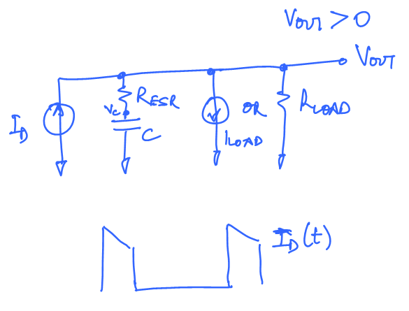
We have the following relations from the above circuit:
Eliminating
$V_C$ in these equations we have:$I_D-I_{LOAD}-{V_{OUT}}/R_{LOAD}=C{R_{LOAD}+R_{ESR}}/R_{LOAD}{dV_{OUT}(t)}/{dt}-CR_{ESR}{dI_D(t)}/{dt}$....(10)Switching State describing equations:
Thus the switching stage transfer function is described by the equations (7),(9) and (10) repeated below:${dI_D(t)}/{dt}={V_{IN}-V_{OUT}(t)(1-D(t))}/L(1-D(t)) - I_L(t){dD(t)}/{dt}$...(7)${dI_L(t)}/{dt}={V_{IN}-V_{OUT}(t)(1-D(t))}/L$.....(9)$I_D-I_{LOAD}-{V_{OUT}}/R_{LOAD}=C{R_{LOAD}+R_{ESR}}/R_{LOAD}{dV_{OUT}(t)}/{dt}-CR_{ESR}{dI_D(t)}/{dt}$....(10)Linearizing the equations
The equations (7) and (9) are non linear as it is evident from the terms where$D(t)$ is multiplied by itself and $V_{OUT}(t)$. Equation (10) is not strictly linear in $I_D$ and $V_{OUT}$ since it does not follow the Zero Input Zero Output rule. We will linearize the equations and then use them to obtain a Laplace transform of the transfer function of the switching modulator to use in our loop Gain calculations:To linearize the equations we will make a small perturbation in the quantities of interest so we have:
$ΔI_D=i_D$, $ΔI_L=i_L$, $ΔD(t)=d$ and $ΔV_{OUT}(t) = v_{OUT}$Putting these substitutions in (7),(9) and (10) and then ignoring the terms where the small perturbation quantities are multiplied with each other we have the following transformed equations:
$si_D={V_{OUT}(t)d-v_{OUT}(1-D)}/L(1-D)-I_L(t)sd$...(11) ----> derived from (7)$si_L={V_{OUT}(t)d-(1-D)v_{OUT}}/L$.....(12) ----> derived from (9)$i_D=v_{OUT}{sC(R_{LOAD}+R_{ESR})+1}/{R_{LOAD}(1+sR_{ESR}C)}$...(13) ----> Derived from (10)Things to NOTE:
- All small signal parameters have 0 initial value. Therefore
${dΔI_D(t)}/{dt}=si_D-i_D(0+)=si_D$ -
$V_{OUT}$,$D$,$I_L$and$I_D$are all large signal values at the state we want to analyze the small signal response -
$v_{OUT}$,$d$,$i_L$and$i_D$are all small signal perturbations over their large signal counterparts.
Voltage Mode control Transfer function
Finally here we can derive the small signal transfer function of the Boost converter switching modulator using the equations we have derived in the last section.Substituting (11) in (13) and simplifying we have:
Here we successfully get the complete transfer function. Here we see the right half plane zero caused by the boost converter architecture given as:
Also the ESR zero is seen. In the denominator we can see the 2 poles created by the LC circuit.
Current Mode control Transfer function
In Current Mode control the feedback directly sets the inductor current as compared to voltage mode control where the feedback controls the duty cycle.There from equation (9) we have:
$d={si_LL+(1-D)v_{OUT}}/{V_{OUT}(t)}$...(14)Use (14), (11) and (13) to eliminate d and calculate
$v_{OUT}/i_L$ we have:So with Current mode control we see that the 2 poles of the LC circuit are now just reduced to a 1 pole caused by a current source and a capacitor circuit. The right half plane zero and the ESR zero remain unchanged.