Here is a list and analysis of compensation techniques, that I have come across/used in my circuit design experience. Compensation can be used to:
- reduce noise (filter it off)
- make amplitude response flat
- make the amplifier stable for a particular feedback configuration
Caution
One thing to always keep in mind when doing compensation circuits is to not get carried away by just poles and zeros. Even if you get all the poles and zeros right and the amplifier bode plot looks very good the circuitry you may have added in the process may not be practical from a transient stand point. For example if you added a cap at a very high impedance point to make a dominant pole and the cap value you placed is so large that when that node needs to respond to a step it is very slow, then that solution may not be usable for compensating that design. Always check transient responses of compensated amplifiers and make sure they are stable and within specificationsDominant Pole Compensation
This technique involves compensating by locating the dominant pole node and making it more dominant by loading it with more capacitance.Advantages:
- Simple to implement
Disadvantages:
- Great deal of bandwidth loss
Gain Compensation
The gain of the amplifier is reduced so that loop gain bode plot moves down and gets stabilized. For an opamp circuit this can be done by decreasing the gm of the input differential pair. Or the Rout of the amplifier can be reduced, this will push the output pole also further which will be good if it is not the dominant pole.Advantages:
- No bandwidth loss
Lead Compensation
This technique basically involves making a feedback network that introduces a pole and a zero in the loop gain but the zero is always before the pole. So this way the zero is placed on the non dominant pole of the amplifier to cancel it off and then the pole introduced by the network becomes the non dominant pole and since it is at a higher frequency the net effect is that the non dominant pole is moved further in frequency without effecting the dominant pole of the amplifier. Mathematically the loop gain is modified to include the following term:where Where
$$|z_1| < |p_1|$$A lead network to do this is shown below:
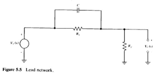
The technique can be best understood by considering the lead network circuit in a feedback system.

The loop gain equation is given as:
here the last term is the open loop opamp transfer function – modeled as a 2 pole system. So we see that if we make the zero $(=-1/{R_FC})$ equal to the non dominant pole
$(=-1/τ_2)$ then out non dominant pole would become $-1/(R_G||R_F C)$ which is higher in frequency than the zero. Hence we have moved the non dominant pole higher up in frequency and stabilized the system. See a more detailed analysis in Op Amps for Everyone, Fourth EditionLag Compensation
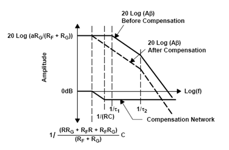
This technique involves placing a pole and then a zero successively much before the non dominant pole of the opamp comes. Since the pole comes first the magnitude response decreases compared to what it was before, also the phase response starts decreasing, when the zero comes the phase response is restored to what it was before as if the pole did not occur. This happens before the non dominant pole. So the net effect is that the non dominant pole sees the same phase response as before but a lesser magnitude response and so the magnitude response crosses the 0 dB line at a lower frequency thus stabilizing the opamp. Mathematically the loop gain is modified to include the following term:where Where
$$|z_1| > |p_1|$$A Lag compensation network is shown below:
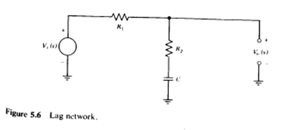
To understand the technique look at the circuit:
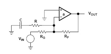
The loop gain bode plot looks like:
Another way to do this is by the following schematic:
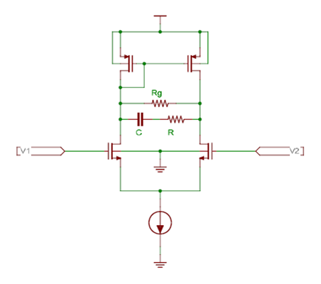
The transfer function of the above circuit is:
So we see a pole is introduced before the zero and we have lag lead compensation. If the differential amplifier had been a fully differential one then also the network would result in lag lead compensation since then the transfer function becomes:
A typical Lag Lead compensation frequency plot is shown below:
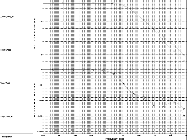
This plot has the pole at the 1KHz and the zero at 3KHz. The gain falls faster than before at 1KHz and the becomes parallel to the original at 3KHz at a lower level. While the phase response recovers fully as if the pole zero pair had not occurred.
Design Tip
As can be seen from the concept that the pole of the lag lead network should be placed much before the GBW of the loop gain before the addition of the network to be effective in increasing the phase margin.Lead-Lag Compensation
Circuit 1
When both lead compensation and lag compensation are used together the system is using Lead-Lag compensation. Mathematically the loop gain is modified to include the following term:Where
$$|p_2| < |z_2|<|z_1| < |p_1|$$Example of such a circuit is:
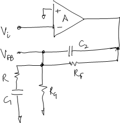
The poles and zeroes for this network are given as:
where K is given as:
If we take some reasonable approximations as discussed in this article we can approximate the poles and zeros to:
The zeros are the same simple values. The poles are:
If
$C_2≪C_1$ and $R≪R_F||R_G$ then we can approximate the poles as:$$p_2≈-1/{RC_2}$$}}}
Circuit 2
Another form that is called the Lag Lead network is:
Where
$$|p_2| < |z| < |p_1|$$Example circuit of this is (the same that we discussed for the Lead Network circuit 2):
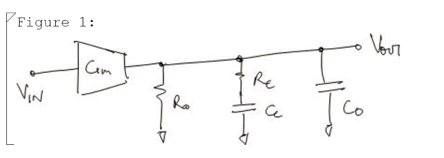
The poles and zero of this network are given as:
If one time constant in the circuit is very dominant than the other then the poles can be approximated as:
Feedforward Compensation
In this method a capacitor is connected across a amplifying stage to remove the stage at high frequencies to eliminate the pole created by that stage and reducing the gain.Dual Pole Compensation
In this type of compensation 2 consecutive poles are introduced in the system at a very very low frequency i.e. . This then causes the gain to drop by 40dB per decade and it drops to 1 very soon without reaching to any significant frequency. The phase however is not 180 deg since that much phase shift due to 2 poles happens only at infinite frequency. So although the phase margin is very small maybe just a few degrees the system can never be unstable since it is free from any parasitic poles. One question can be what about ringing response. Since the Bandwidth and GBW of the system is so low, no visible frequency can pass through it so no ringing will be observed.Advantages:
- Simple method
- Does not require attention to parasitic poles
- No ringing problem
Disadvantages:
- Can only be used for systems working for DC voltages
- Very slow response
Miller Compensation
In this type of compensation a capacitor is placed across a negative gain stage causing the miller multiplication of the capacitance on the input side making that the dominant pole.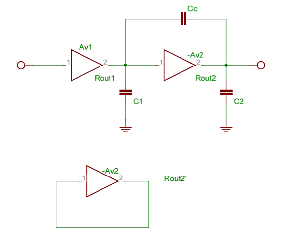
Here if Rout2’ < Rout2 then the output pole is pushed further away. The miller cap acts as a short at high frequency thereby pushing out the pole. After compensation the equivalent circuit looks like:
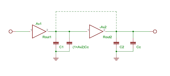
Before Compensation the pole locations are:
After compensation the poles become (approximately):
where $R_{out2}'$ is the output impedance of the second stage when the output is shorted to its input. To see a detailed derivation of the above see here
Coming Soon Nested Miller Compensation
See Also
- The book Frequency Compensation Techniques for Low-Power Operational Amplifiers (The Springer International Series in Engineering and Computer Science)
has good chapter on compensation analysis of multi stage opamps.
- The book Op Amps for Everyone, Fourth Edition
has a good chapter on different networks for compensating opamps
- Lead Lag Network
- Miller Compensation Derivation
- Lag Lead Compensation