Getting Familiar with a Process

20 August 2019 Link


Getting Familiar with a Process Checklist

Get Information about the Process

  1. Get the list of all devices available
  2. Get the cross sections of the process and all devices to get visualization of:
    1. Parasitics
      1. Resistances
      2. Diodes
      3. BJTs
      4. Capacitances
    2. Latchup Possibilities
    3. Breakdown Issues
  3. Get the Specification limits of the parameters of the devices as detailed below:
    1. MOS Devices
      1. Electrical Parameters
        1. gm/Id vs Id/(W/L) Graphs
        2. VTH
        3. Rdson*area
        4. Qg*Ron
        5. BVdss
        6. BVox
        7. Idsat (Velocity Saturation current)
        8. Isub/Id
        9. Maximum Operating Voltage (MOV)
        10. Absolute Maximum Voltage (AMV)
        11. Matching Constant
      2. Physical Parameters
        1. Oxide thickness
        2. Dimension Limits
    2. BJT Devices
      1. Electrical Parameters
        1. Is/Vbe
        2. Ft
        3. Beta
        4. Va
        5. BVebo
        6. BVcbo
        7. BVcso (collector to substrate if present)
        8. Vbe matching constant
        9. Rc (collector resistance)
        10. Ikf (current at which beta becomes half)
        11. Vce-sat (normal saturation voltage)
    3. Resistors
      1. Electrical Parameters
        1. Resistance per square
        2. Temperature coefficient of the resistors
        3. Matching coefficient
      2. Physical Parameters
        1. Dimension limits
    4. Capacitors
      1. Electrical Parameters
        1. Capacitance per sq um
        2. Temperature coefficient of the resistors
        3. Matching coefficient
      2. Physical Parameters
        1. Dimension limits
    5. Metals
      1. Electrical Parameters
        1. Electromigration current limit table (vs temperature) for each metal layer
        2. Resistivity of the metal layer per square
      2. Physical Parameters
        1. Thickness of each metal layer
  4. Get the layout design rules for the process.
  5. Get the process PDK usage information for the devices

Study the Process

Try to memorize as much as you can in this section since it comes in handy all the time.

Layout

  1. Go briefly over layout design rules and identify any points that may need to be considered for circuit design.
  2. Generate a sample layout of all the allowed devices on a single plot to get relative sizes of the devices.
  3. For p-substrate chips is p+ automatically inserted by the tapeout program or does it have to be done manually?

Electrical

  1. Assemble all device data in your design spreadsheet
  2. Find out if the Bipolar devices are properly modeled for saturation region or at least the model knows when the transistor goes into saturation.
  3. Create the device characterization schematics and simulate them over corners and verify electrical parameters
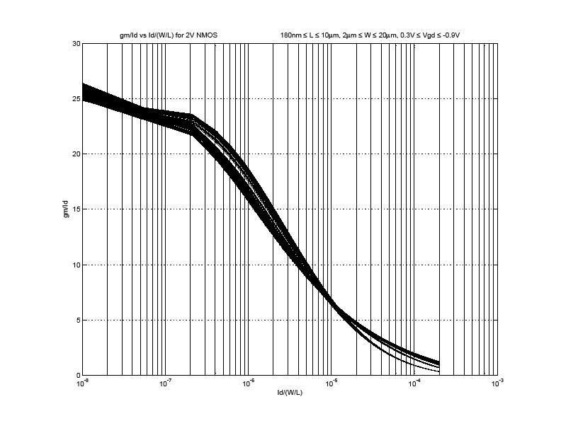
  4. Create the gm/Id vs Id/(W/L) semi-log graphs for the MOS transistors of the process. For Cadence the process is described here Getting gm by Id vs Id by W by L graphs in Cadence. A typical graphs looks like as follows:
  5. For a BiCMOS process do a comparison between bipolar and MOS current mirror match. Do an area comparison for mirrors with the same matching.
  6. Do an analysis if having resistor degeneration in MOS produces better matching with less area compared to just sizing up the MOS device.
  7. Do rough simulations to compare the Ballpark Numbers numbers for the process.

Miscellaneous

  1. Create a process caution list to be followed, for example if the process does not have isolated devices then analog blocks should be created with proper isolation with guard rings, and things like this, etc.