Circuit
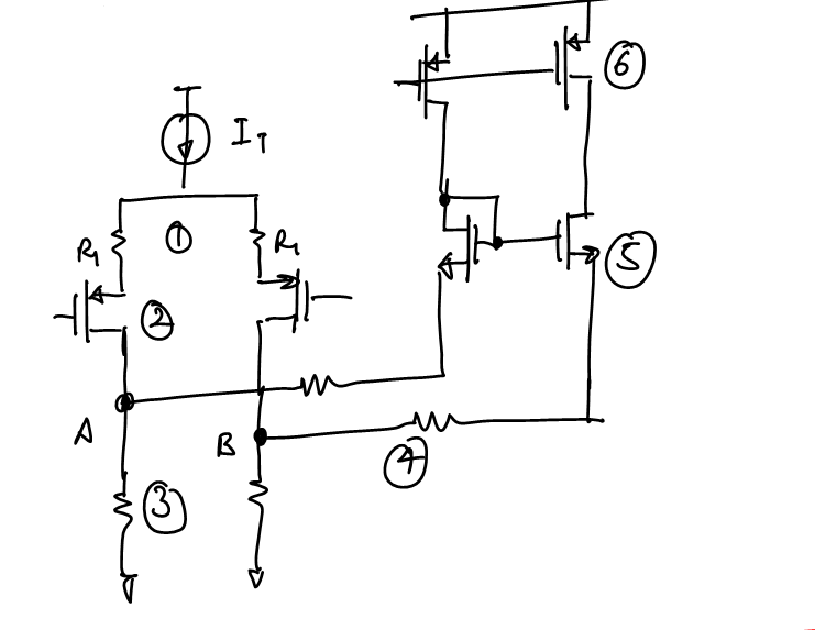
The general circuit is taken as:
The circuit above shows a general circuit for the folded Cascode MOS diffamp. $R_1$ are degeneration resistors, $R_4$ are degeneration resistors for the fold transistors. Each component pair has a number and contributes to the input offset of the diffamp. Here we calculate the offset contribution due to each matched pair component and then take the root of sum of squares of all the contributions to get the actual offset. For each component the mismatch delta is the sigma of the mismatch, so the final offset is the sigma of the offset.
Offset Contributions
Input degeneration resistors
For these resistors, any mismatch in then causes a delta drop due to the tail current which would have to be balanced out in the input thus looking like an offset:where
$g_{m2}/{1+g_{m2}R_1}R_1$ is the gain from the input to the source of the input pair of the diffampThis gives us:
where
$G_m=g_{m2}/{1+g_{m2}R_1}$ is the transconductance of the input pair with the resistor degenerationInput transistor pair
The input transistor pair offset contribution can be taken directly as the$V_{th}$ (or $V_{be}$ for bipolar input) mismatch number. ThusLoad Resistor
When the load resistor pair has a mismatch the input has to be adjusted so as to distribute the tail current on them in such a way so that the resistors have the same voltage drop. So we have:Solving this for
$V_{os3}$ we getIf we had a MOS load then
$V_{os3}$ would simply be:where
$ΔI = {2ΔV_{th} }/{V_{dsat} }I_T/2$ is the current mismatch of the MOS current sinksCascode Degeneration Resistor

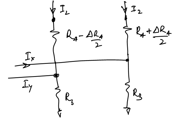
This image above shows the effect of mismatch of the cascode degeneration resistors. We can write the equation to calculate
$I_y - I_x$ as follows:Solving this we have:
So we can calculate
$V_{os4}$ as:Cascode Transistors
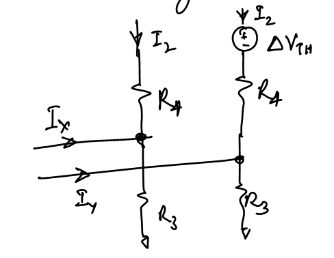
The$ΔV_{gs5}≃ΔV_{th5}$ of the cascode devices can be considered as a voltage source in series with $R_4$ as shown below:
We can write the equation again to find
$I_x-I_y$ as:Thus we have:
Now as we did before we can write the offset contribution
$V_{os5}$ as:Active MOS load

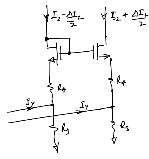
Assuming 0 body effect on transistors M5 due to mismatched currents since the mismatch current difference is usually too small to cause any significant threshold voltage change between the devices
We can write the equation to calculate
$I_x-I_y$ as:Here
$ΔV_{gs5}={ΔI_2}/g_{m5}$So we have:
and so
$V_{os6}$ can be expressed as:where
$ΔI_2 = {2ΔV_{th} }/{Vd_{sat} }I_2$ is the current mismatch of the MOS current mirror.Final Mismatch
The final mismatch is just the root of the sum of squares of the individual mismatches since all mismatches are uncorrelatedReferences
- Opamps
- Books: