Explanation
Did some exploring on why the LX node shows ringing when switching. Basically the reason is the parasitic capacitance on the LX node and the stray inductance in the path of the power switches driving the LX node as shown in the diagram below:
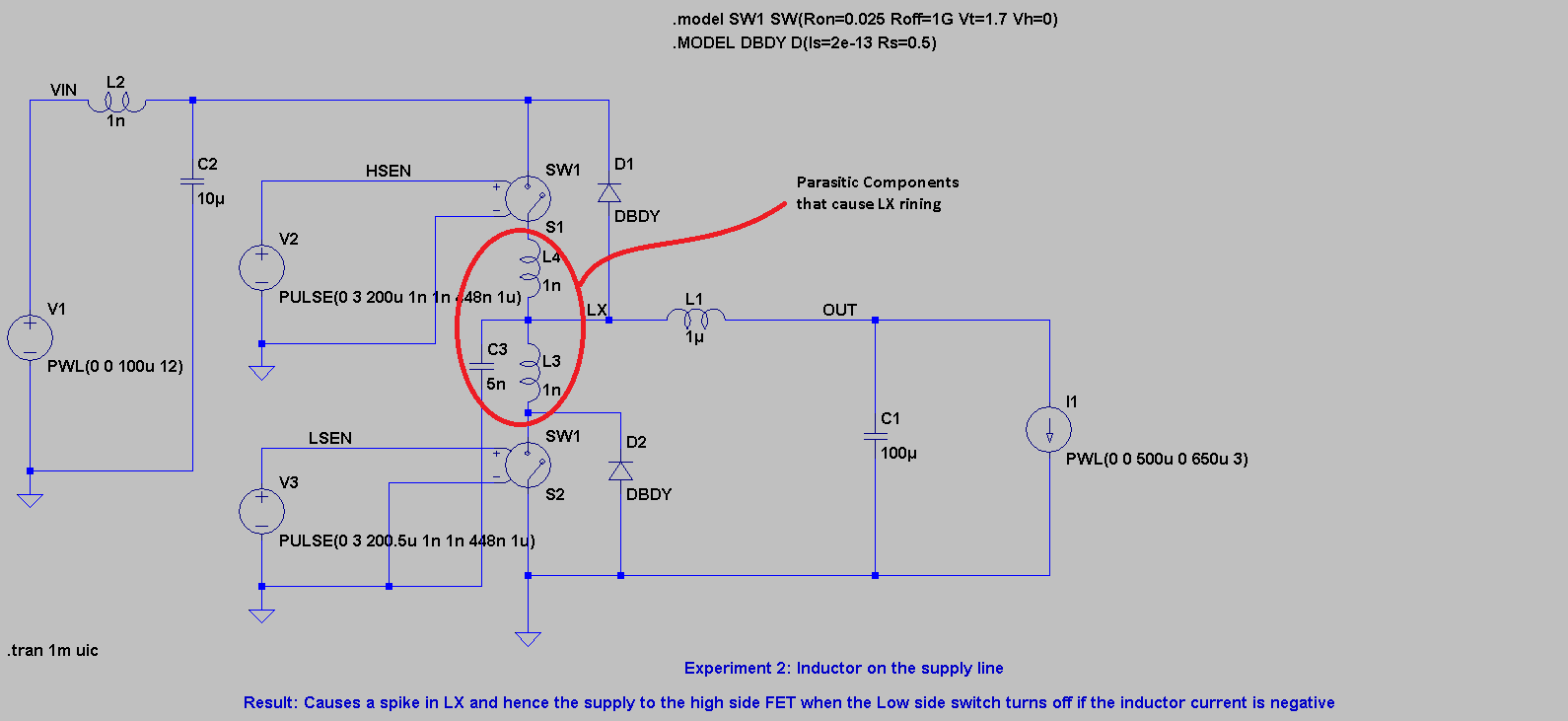
When the LX needs to go from 0 to Supply the parasitic LX cap needs to charge fast and that current is built up in inductor L4 and when the cap is charged to Vin the inductor in L4 needs to change to a low value very quickly thus overcharging C3 and causing the ringing. The same thing happens for when LX needs to discharge to 0V and the current needs to change rapidly in L3. Which is when LX rings after coming to ground.
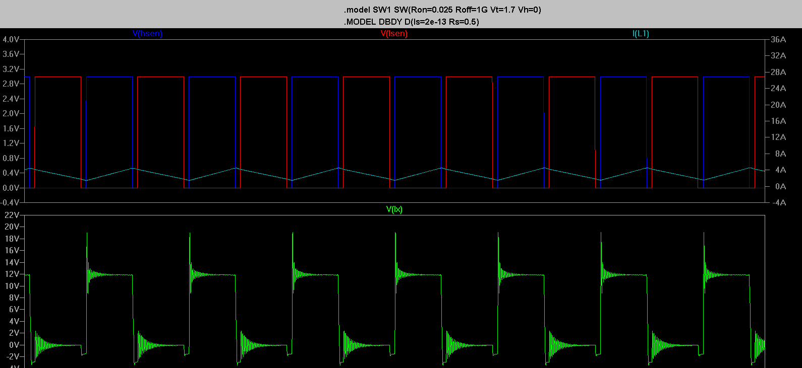
The ringing is seen as:
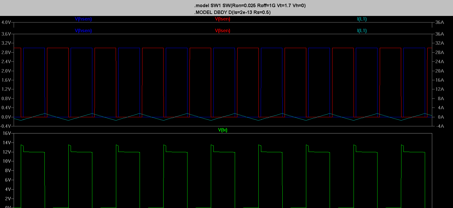
If we remove the capacitor the ringing disappears since there is no initial big current needed to charge the node and the waveform is:
If we just remove inductor L3 the low side ringing disappears as shown below:
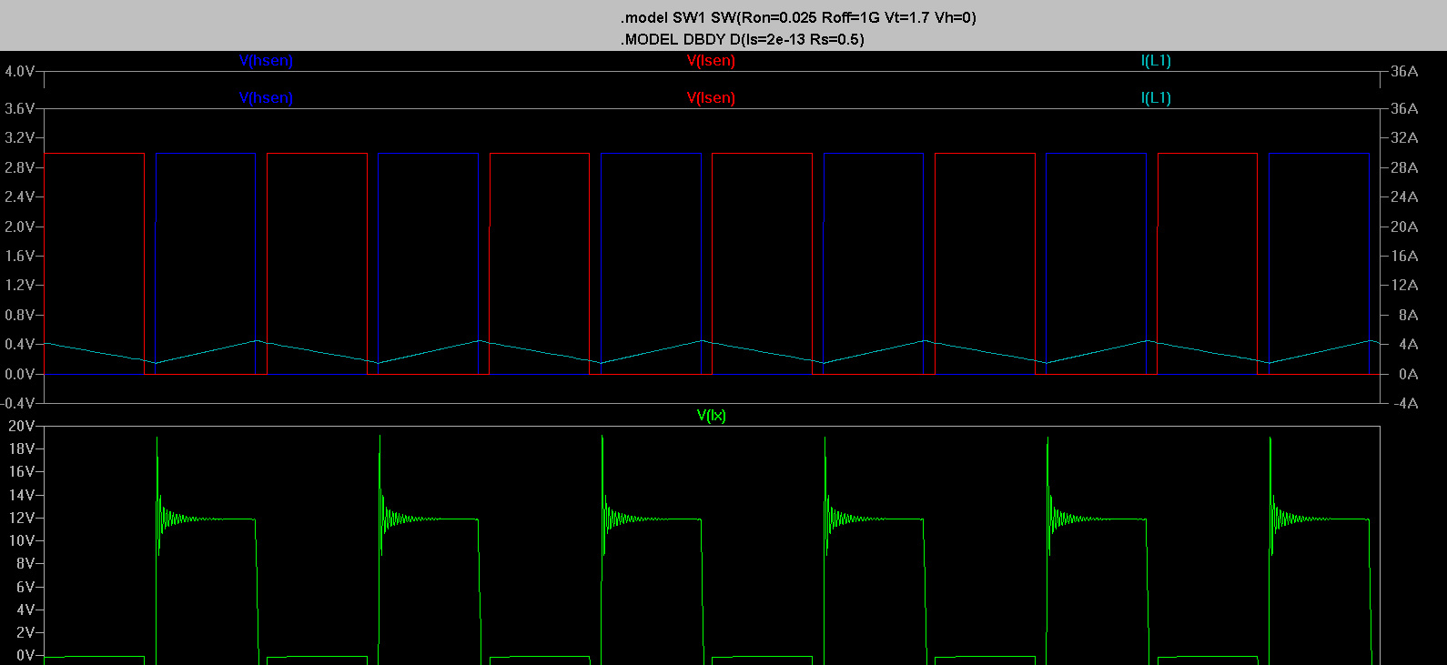
and finally if we just remove the inductor L4 the high side ringing disappears as shown below:
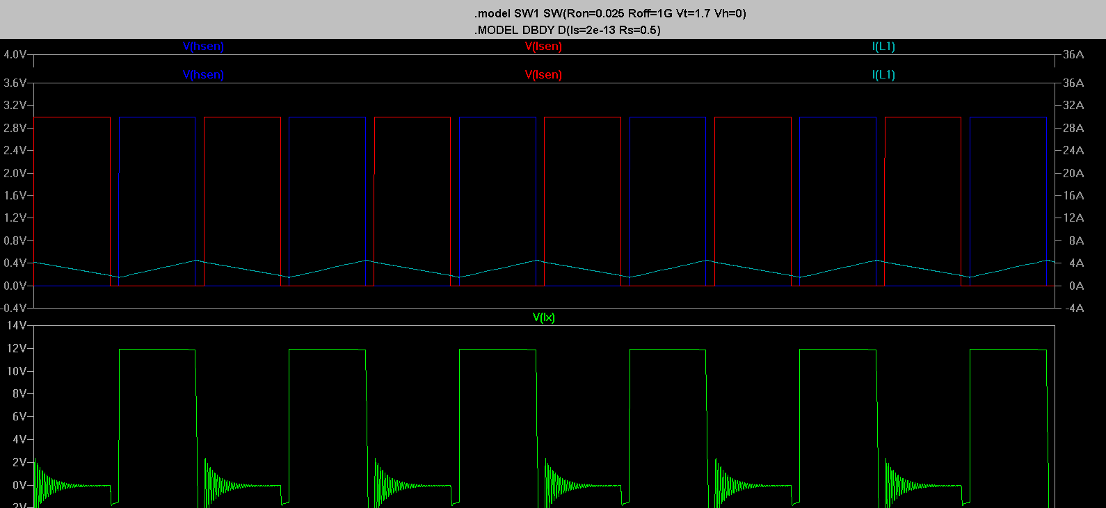
Also the ringing will also be there if there is an inductance in the supply or ground connection from the FET i.e any parasitic inductance from the supply Cap (Cap to supply or Cap to PGND) to the LX cap will cause the ringing.
References
- The LTSpice schematic for this experiment is here