Amplification mode
Here we derive the impedances as seen looking into the terminals of a MOS device connected in amplification mode. The setup is as follows: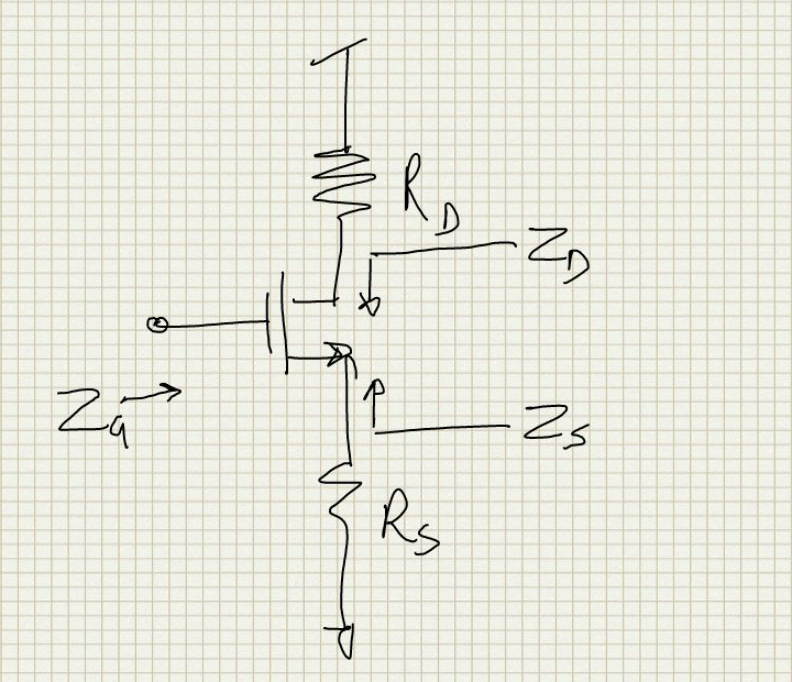
Gate Impedance
The DC impedance looking into the gate is practically infinite since the gate leakage is very smallDrain Impedance
The small signal circuit to derive the drain impedance is as follows: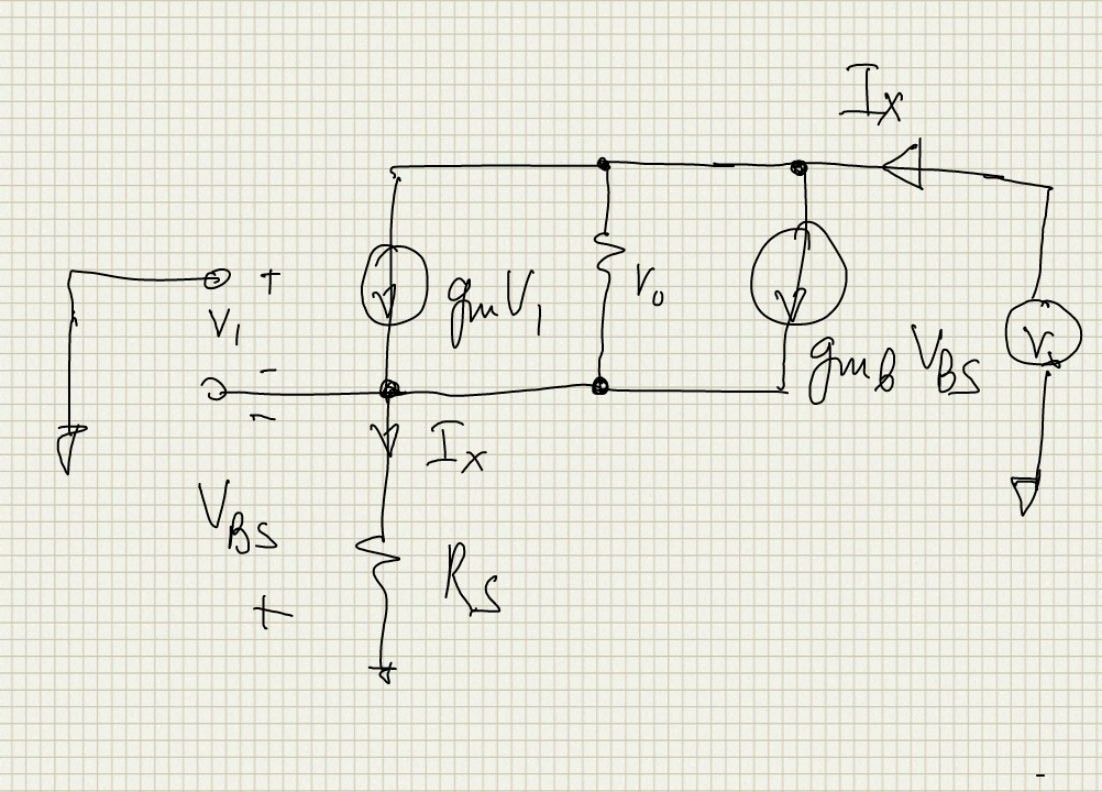
We can write the KVL from the test source to ground through Rs and from gate to ground through Rs we have the following 3 equations:
Eliminating
$V_1$ and $V_{BS}$ and solving for $V_x/I_x$ we haveSpecial Cases:
- If
$g_m≫g_{mb}$and$r_og_m≫1$and$R_Sg_m≫1$then the expression simplifies to:-
$$Z_D = r_oR_Sg_m$$
-
- If
$R_S=0$then-
$$Z_D = r_o$$
-
Source Impedance
The small signal circuit to derive the source impedance is as follows: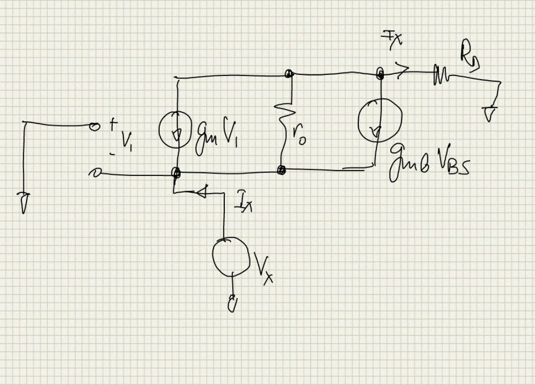
Again writing the KVL from
$V_x$ to the gate and to the drain we have the following equations:Eliminating
$V_1$ and $V_{BS}$ and solving for $V_x/I_x$ we haveSpecial Cases
If$R_D=0$ thenDiode Connected Mode
Here we derive the impedances as seen looking into the terminals of a MOS device connected as a diode. The setup is as follows: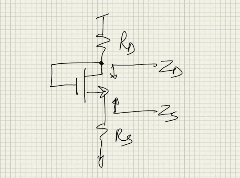
Gate-Drain Impedance
The small signal circuit to derive the Gate-Drain impedance is as follows: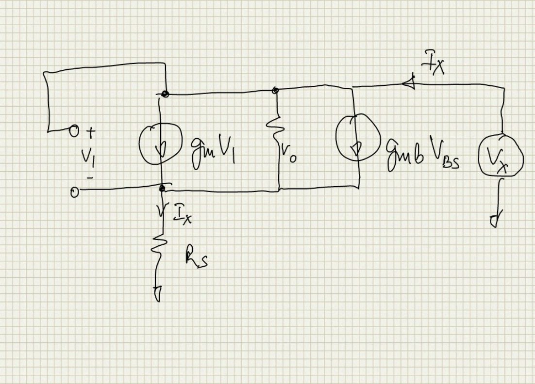
Writing the KVL through the
$V_1$ loop and through the $r_o$ we have the following equations:Eliminating
$V_1$ and $V_{BS}$ and solving for $V_x/I_x$ we haveSpecial Cases
- If
$R_S=0$then the expression reduces to-
$$Z_D=r_o∥1/g_m$$
-
- For
$r_o→∞$and$g_m ≫g_{mb}$then the expression reduces to:-
$$Z_D=1/g_m+R_S$$
-
Source Impedance
The small signal circuit to derive the Source impedance is as follows: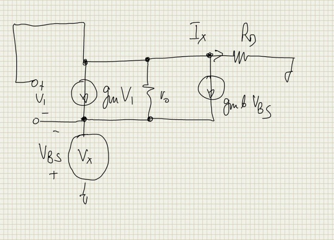
Writing the KVL through the
$V_1$ loop and through the $r_o$ we have the following equations:Eliminating
$V_1$ and $V_{BS}$ and solving for $V_x/I_x$ we haveSpecial Cases
- If
$R_D=0$then the expression reduces to-
$$Z_S=r_o∥1/{g_m+g_{mb}}$$
-
- For
$r_o→∞$and$g_m ≫g_{mb}$then the expression reduces to:-
$$Z_D=1/g_m+R_D$$
-
Reference Books
- Design of Analog CMOS Integrated Circuits
- Analysis and Design of Analog Integrated Circuits
- CMOS Analog Circuit Design