In this article we discuss in detail about matching of devices in circuits with some supporting derivations.
Test Data Usage
From process runs the measured values like Vbe, Vth, size differences are all measured for each run and this data should be available. If this data is available we can plot a distribution function and calculate the mean of the data over a period of time and also the standard deviation from the mean for that particular parameter. 6 times the standard deviation can be taken as the mismatch number according to the yield number required. For example if the mean of Vbe measured over a 1 year period in all the process runs of the transistor is 0.7V and the standard deviation is 1.8mV then probably we can take dVbe=10.8mV and this would ensure maybe 99% of all samples lie in this standard deviation range thus making our yield for the target design as 99%. (Even though 6 sigma corresponds to > 99.999% the six sigma we calculate here may not be the true sigma since it is of a limited number of samples)The modelling reports usually give the mismatch data as a Pelgrom curve as shown below:
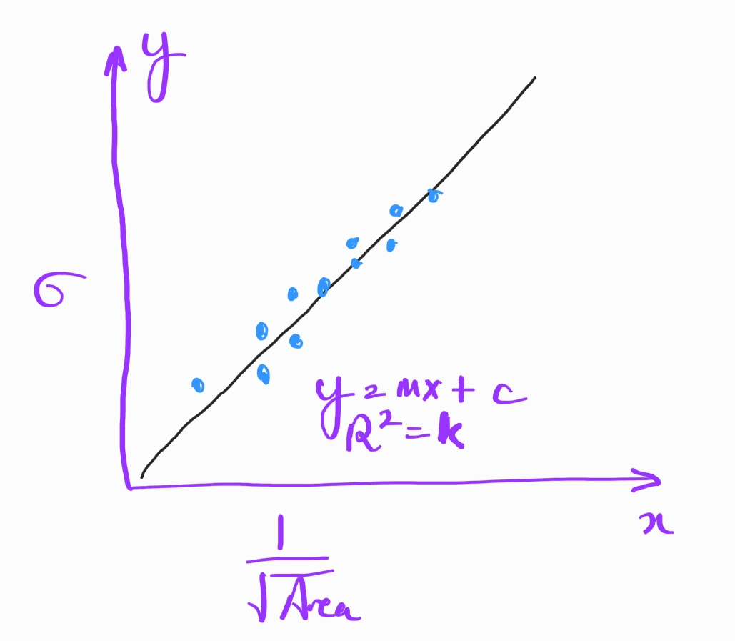
Here y axis is the sigma of the mismatch parameter and x axis is the 1/sqrt(area).
The measurements are done and then a straight line is derived to best fit the measured data. The equation of the line is given and the
$R^2$ parameter which is the statistical determination on how close the best fit line fits all the samples. See some info about it hereMOS Matching
A MOS device may be used where the matching of Vgs is important or where the matching of drain currents are important. Both have different design requirements as seen below.Matching Vgs
If 2 matched transistors operate at the same drain current then the Vgs mismatch of the transistors can be expressed as:Differentiating this and putting
$dI_D=0$ we have:Where the symbols have the usual meaning and
$S=W/L$. So we see to minimiz $dV_{gs}$ we must minimize the overdrive voltage, i.e. increase the W/L ratio of the transistors or decrease the current through the transistors. Matching Ids
Simple MOS Mirror
If 2 matched transistors have the same Vgs (Current Mirror) then the Current Mismatch can be calculated as:Differentiating this and putting
$dV_{gs}=0$ we have:So we see to minimize the mismatch between currents the overdrive voltage must be maximized, i.e. increase the current going through the transistors or decrease the W/L ratio of the transistors, making Vdsat ~0.3V(preferably 0.5V) is good for current matching.
Also Note that if a transistor goes into subthreshold that degrades the current mismatch since the vdsat is very low or the gm is so high that even small delta vth creates a big current error.
Since
$dV_{th}=K/√{WLm}$ where K is the matching coefficient for a process and m is the multiplication factor in the size and $V_{dsat}=V_{gs}-V_{th}=√{ {2I_{ds}}/{μC_{ox}{mW/L} } }$ in saturation we can put this in the above current mismatch equation to get:Thus we see that the matching can be improved by either increasing the current or increasing the length L of the transistor.
MOS mirror with degeneration resistors
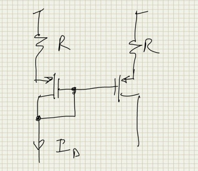
As seen in the above circuit the MOS mirror adds source degeneration resistors so now the equations become:
Differentiating this and putting
$dV_{gs}=0$ we have:Also we have:
Differentiating this we have:
Substituting this in the above equation and evaluating for
${dI_{ds}}/I_{ds}$ we have:If R=0 then this reduces to the expression we derived for a simple mirror.
The minimum for this expression will happen when
${2I_{ds}}/(V_{gs}-V_{th})$ which is the $g_m$ for the MOS device is as low as possible and R is as high as possible. This is a bit counter intuitive if we have the thought process that we should have the gm of the NMOS should be as high as possible so that we can equalize the voltages on the resistors better just like we want to do when we design a cascode mirror. But the cascode and this scenario is different. The cascode's main function is to equalize the drain voltages of the mirror transistors so have a high gm helps because the mismatched currents will still produce the same cascode Vgs and hence keep the drain voltages of the mirror the same (compared to a low gm cascode where different currents will produce larger vgs difference). But here the MOS devices are added to probably create an active mirror or to mirror out the current. The best matched load will be the resistors by themselves but when we add these MOS devices we degrade the matched load to get the mirror out. So here we add the MOS but we need those MOS to also act as good matched loads and low gm is the criteria that must be met for that like for a simple MOS mirror.If we have:
Then we can approximate it as follows:
So a good design practice is to make the
$V_{dsat}$ of the MOS device much smaller than the drop across the resistor for the resistor accuracy to be reflected in the mirror accuracy. Because once we ensure that the $dV_{th}$ is reduced by dividing it with the drop on the resistor and what remains is the resistor mismatch.MOS mirror in subthreshold with degeneration resistors
Since we already saw that it benefits us by making the MOS$V_{dsat}$ lower to better match the currents in a resistor degenerated MOS mirrror subthreshold seems to be the appropriate place where those devices will be biased. The MOS behavior is exponential in subthreshold so we can look at how it affects our mismatch calculation.Here n is the subthreshold factor for the MOS device usually in the neighborhood of 1.4 which can be easily determined from a
$g_m$ simulation or looking directly at the model file. Differentiating the above equation we getSubstituting
$dV_{gs}$ from above and evaluating for ${dI_{ds}}/I_{ds}$ we get:Again now if
$${I_{ds}R}/{nV_T}≫1$$ we can reduce the mismatch equation to:N to M Matching
In this section let us explore what is the matching when say a current mirror is created from a N multiple device to a M multiple device. If$I$ is the current of a unit device and $I_N=NI$ is the current in the Nx device when the the Mx device current ideally is $I_M=MI=I_NM/N$.Now with Mismatches we have:
Here the
$1/√2$ factor comes in because ${dV}_{th}$ is the standard deviation of the difference as defined here. Also note that the input current $I_N$ is fixed and is provided as input but the input transistors will redistribute the total given current among themselves due to mismatches and that is why we have to take into account the mismatch variations of the input transistor array as well.Similarly for
$I_M$For the underlying process the means scale ideally:
To look at the mismatch of the current from the ideal scaled current we take the difference of
$I_N$ scaled with $I_M$ we have:Also transconductance of the unit device is the same on both sides:
Putting this in the previous equation, we have:
The above equation tells us how to adjust the mismatch sigma of 2 similar size devices when trying to calculate the mismatch between an ideal scaled current and the resultant current. So if we have forced
$I_N$ and want to scale it by $M/N$ then the sigma of the error of the scaling is calculated by adjusting the sigma of mismatch of 2 identical devices by the factor $√{1/{2N}+1/{2M}}$The LTspice file here verifies this derivation. The current would have to be exported and then the standard deviation difference can be calculated in a spreadsheet.
Another question to consider is that what is the distribution of the
$I_M$ current given a $I_N$ current. We can rearrange the last equation above to give us:So we see the mean as
$I_NM/N$ while the sigma is still the same as above.Resistor Matching
Mismatch between Series-Parallel Resistor networks
Here we try to find out the relation of matching between 2 resistor networks that consist of a series/parallel combination of some unit segment resistors to the matching between the unit segment resistors themselves. Let us suppose that the matching between the unit segments is given as:where W and L are the unit segment dimensions and
$A_R$ is the matching coefficient of the resistors. So now suppose we have the following simple network with 2 resistors in series. Each resistor is the unit segment resistor.
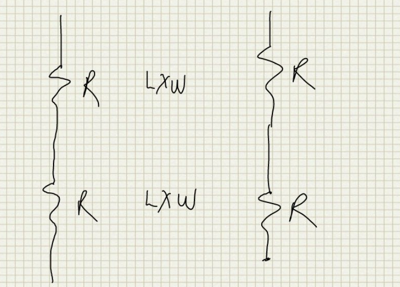
If we just consider the total area on each network we have the following matching expression:
since each side now has 2 times the area of the unit segment
The alternative way to solve it right from the basic principles is to assume each pair as a separate matched pair and to find the matching of the system by adding powers of the mismatches of individual components since the mismatch is uncorrelated. So supposing mismatch in just the upper pair as shown below:
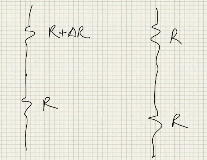
So we have:
Same contribution from the other pair and so the total mismatch is:
And so the mismatch ratio is:
This is the same result we got when we just considered the total area on each side which was the intuitive easier method
Now consider the following simple network with 2 unit segment resistors in parallel:
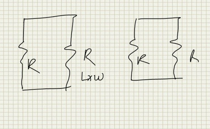
Again if we just consider the total area on each side we have the following mismatch expression:
Again we can solve it using the basic principles and considering each matched pair separate and combining the uncorrelated mismatch factors. The mismatch of one pair is shown below:
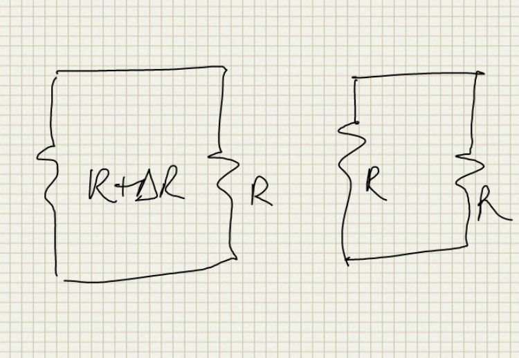
So we have:
Same contribution from the other pair so the total mismatch of the network is given as:
And so the mismatch ratio is:
Which is again the same as the result we got by just considering the total area.
Also we see that it does not matter how the resistors are connected the final mismatch only just depends on the area on each side. Hence we can just use the total area on each side to figure out the total mismatch of the resistor network.
Accuracy of a resistor divider
In IC Design we implement resistor dividers as a multiple of the same segment resistors for better matching. Here we derive an expression to quantify the accuracy of the resistor divider i.e. the error in the output voltage as a result of the mismatch between the segments.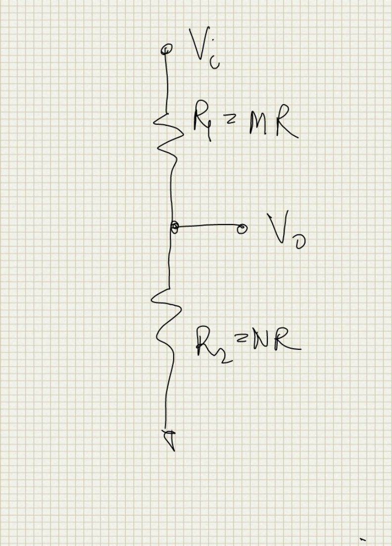
We have:
For variation in
$R_2$$V_{O1}$ due to $R_2$ variation only is:For variation in
$R_1$$V_{O2}$ due to $R_1$ variation only is:Since both are uncorrelated we have:
Note here dR is the absolute variation in the sigma and not the sigma of the difference of 2 side by side R. To convert the mismatch sigma of R to dR used here divide the sigma of the mismatch by
$√2$, See Standard Deviation difference for explanation about this.BJT Mismatch
Matching Collector Currents
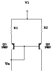
The Mismatch of the collector currents of this mirror can be derived as follows:
differentiating this:
We know that:
Differentiating this we have:
Dividing (1) by
$I_C$ and substituting this we have:Taking the
${dI_C}/I_C$ term on one side we have:For small R or R=0
$dV_{be}=0$ then mismatch is given by:For an ordinary bipolar mirror the collector current mismatch will be the same as the IS mismatch which may be 5 to 10%. For large R the
${dI_S}/I_S$ term is reduced (divided by R) and the mismatch depends on the R mismatch and $α$ mismatch.NOTE: For missirs without base current error compensation the base current will cause and error also. Above the left branch will have the collector current plus the base currents of both the transistors.
See Also
- Standard Deviation difference - A derivation to see how the standard deviation of a parameter is related to the standard deviation of the difference of the parameter between 2 identical elements.