Description
This is a motions sensing light installed outdoors to turn on the light as soon as motion is detected. It is a very old model which was already installed in my 1961 house when I bought it. The light kept working in the day time as well. I replaced the light with a new one and decided to open it up and find out how it works and fix it up. From the outside the like looks like: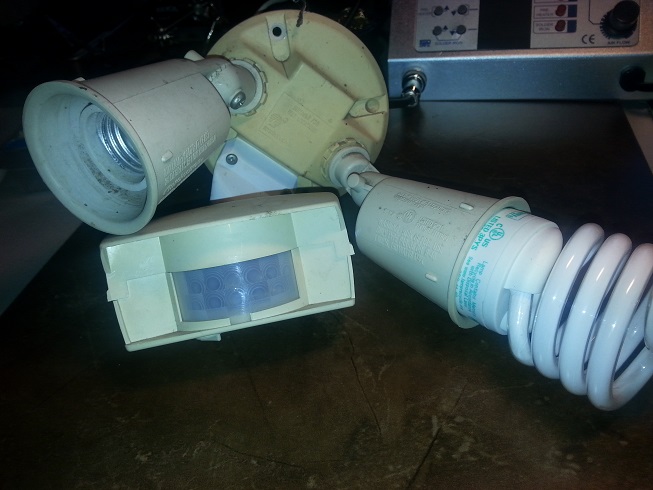
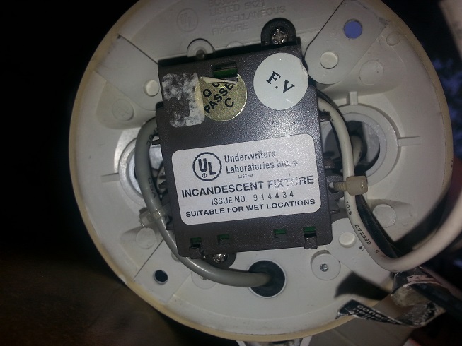
Turning it over, from the back it looks like:
Internals
The back module is a single module that steps down the AC and provides power to the circuit board in the front light and motion sensing module. I did not open the back module since it was working fine and the circuit board was receiving about 22V.On opening the front module I see the circuit board:
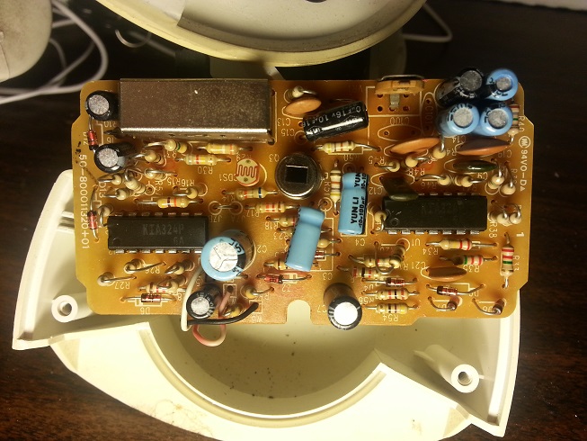
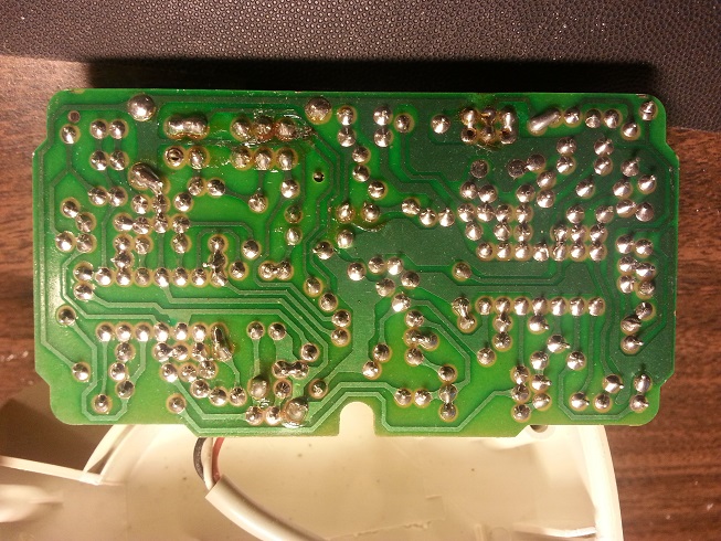
It is a very discrete design! Lots of components which really means it is an old product. It is a single sided PCB with components on 1 side and all connectivity on the back side as seen here:
Circuit
I traced out the circuit of the PCB and here is the sketch from my Galaxy Note 2, I didn't have time to make it pretty: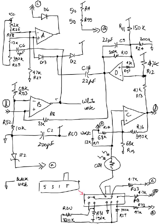
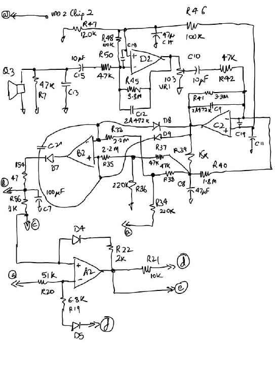
From the front module 3 wires come to the PCB:
- Red Wire - Supply +ve of 22V
- Black Wire - Ground
- White Wire - High/Low signal from the PCB to turn ON/OFF the light
Q3 on page 2 is the motion sensor (datasheet linked below). CDS1 is a LDR (Light Dependent resistor). The 2 ICs seen in the PCB front picture are quad opamp ICs KIA324P. The one on the left side is 1 and the one on the right side is 2 (i.e. A2,B2,C2,D2 are opamps from IC on the right side on the PCB picture). The zener Z2 is a 8.3V zener providing supply rail to the second IC.
The circuit looks straightforward. D2 and C2 form amplifiers to gain up the signal from the motion sensor by about 5000 (70 each). The output of C2 charges up the capcacitor C21 connected across the inputs B2. With sufficient charge time on C2 output of B2 will go high and charge the 100uF capacitor C7 making +ve terminal on A2 high making (e) and (d) high. (d) high makes output of B comparator high i.e. the White wire to the back module. During the day time when the LDR resistance is low (f) is high causing the output of comparator D low preventing the white wire from going high. Comparator A I think does some discharge function during the night or day boundary. The switch changes the discharge resistor for Capacitor C7 to change the ON time of the light.
D2 +ve biasing voltage seems to be 0V. The IC works for 0V input voltage easily but the network on the +ve terminal on D2 is a bit strange. It seems that it is getting the bias from its -ve terminal and applying that same bias on +ve terminal of D2 and C2.