On This Page
Specifications to Consider
- Supply Current
- Low to High Propagation Delay
- High to Low Propagation Delay
- Offset
- Minimum Supply Voltage for Operation
- Common Mode Rejection Ratio (Opamps Only)
- Power Supply Rejection Ratio (Opamps Only)
Design and Simulation parameters
- Input Common mode range or input dynamic range
- Output Dynamic Range
- Offset analysis by Monte Carlo
- Minimum Supply Voltage
- Opamp Specific
- Stability - Loop Gain, Phase, Gain Margin, Phase Margin, Bandwidth, Gain Bandwidth Product
- For different input levels
- For different outputs/loads
- Step response (Settling time and ringing)
- PSRR from supply and substrate
- Small Signal
- Different Supplies
- Different Loads
- Step Response
- Different Supplies
- Different Loads
- Small Signal
- CMRR
- Small Signal
- Different Input levels
- Step Response
- Different Input Levels
- Transconductor Specific
- Small Signal
- Transconductance as a function of input common mode
- Maximum Source and Sink Currents
- Input range with 5% degradation on transconductance in either direction
- Comparator Specific
- Propagation Delay for a small overdrive input voltage at different common mode inputs
- Input Low to High
- Input High to Low
- Propagation Delay as a function of overdrive input voltage at different common mode inputs
- Input Low to High
- Input High to Low
Biasing
- Its better to bias the Opamp using a PTAT current because:
-

- where It is the biasing tail current and gm is the input Diff pair gm for a MOS input Opamp. For a BJT input Opamp gm is proportional to It.
- So in any case by having a PTAT current biasing we will have an increasing gm with respect to temperature. Although the open loop gain does not change but this will be beneficial since the gain bandwidth product which is given by gm/Cout, i.e. which is generally proportional to gm will not decrease with temperature.
- Gain Bandwidth Product is more important since that’s the Bandwidth limit when Opamp is used in feedback. Gain is anyhow very high to make any difference.
-
Stages
- Considerations for designing the input stage are:
- Offset Voltage
- Have high gain with diff pairs to reduce final systematic offset
- Poles
- Gain
- Power Consumption
- Common Mode Rejection Ratio
- Common Mode Swing
- Offset Voltage
- General Considerations:
- Power Supply Rejection Ratio
- Stability
- Output stage design considerations:
- Slew Rate
- Removing body effect on input MOS diff pair can lead to slow down for a sharp transition since now the virtual node has to be charged (input PMOS, input rising) or discharged (input NMOS, input falling) before a valid state can be provided by the diff pair.
- Voltage Swing
- Slew Rate
Comparator Design Tips
- The fastest delay chain is one with successive drive capability of "e" of the successive stages.
- For figuring out the current requirement for a comparator design, you first need to know what kind of capacitance your stage has.
- Like if the drain/collector nodes for a process are like 10fF then to drive them +/-2V in time say 1us you need I = 10f*2/1u=20nA.
- This would give you a stage with at least 0.5us (time taken to reach 0). Now you need a gm stage which gives you 20nA with the desired overdrive say 10mV so you need a Gm of 20n/10m = 2uS.
- Then generally always your MOS input pair is in subthreshold or you may be using BJT for BJT the Gm is Ic/Vt and for MOS it is Ic/(nVt) where n is easily derived from model file as 1+Cd/Cox generally 1.5 is a good number for hand calculation
- So you can figure out Ic = 2u*1.5*25.9m = 77nA is the minimum tail current you need.
- When choosing the topology it is better to give some thought on whether to put resistor load or current source load. This is discussed below in the Folded Cascode section
Caution List
- If one input of the (p input) comparator is connected to a reference like bandgap and the other input is connected to like 5V (overdriven) then the gate of the 5V connected has a reverse Vgs that shifts its Vth by a few milli volts to several milli volts. To prevent this its better to keep the inputs to the comparator clamped close to each other.
Opamp Design Tips
General Tips
- When using bipolar input stage:
- Always protect them for possible BVebo violations.
- Always compensate the Input base current on both input by the same impedance.
- Make sure that they never go into saturation (The input range is appropriately limited or the load drop is low enough) or the opamp/comparator may go into Phase Reversal and not give a valid output.
- To explain phase reversal consider the circuit below:
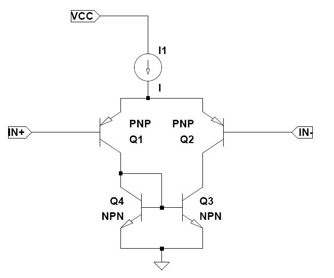
- If the IN+ terminal is the input and is taken to ground transistor Q1 will go into saturation and start leaking current from the collector to the base. This would cause the voltage on the collector of Q1/Q4 to effectively be less than what is expected and it can easily be less than the voltage on the collectors of Q2/Q3. So even though the polarity of the output should be collector of Q1/Q4 > collector of Q2/Q3 we have a reverse situation and this is what is phase reversal. This can also be interpreted as having a very large offset at the input due to drastic reduction in gain by the bipolar going into saturation.
- If we have a single stage as above made of MOS usually we think the input pair Gm should be as high as possible and we want to put it in subthreshold by making the W/L as large as possible. For that it is tempting to make L as low as possible but that starts hurting when the ro decreases since the gain of this stage depends a lot on the ro of the input pair since that is less compared to the active mirror. Saw this in the opamp for the driver supply.
- When Hysteresis is not that critical then don't bring an additional reference line to create it. Just create it inside the block using something like Vbe/Vgs/delta Vbe/delta Vgs/Drop on resistor.
- When using Miller across multiple stages always make sure the miller loop is pre-biased and settles before the main loop starts up to ensure stable startup.
Folded Cascode Tips
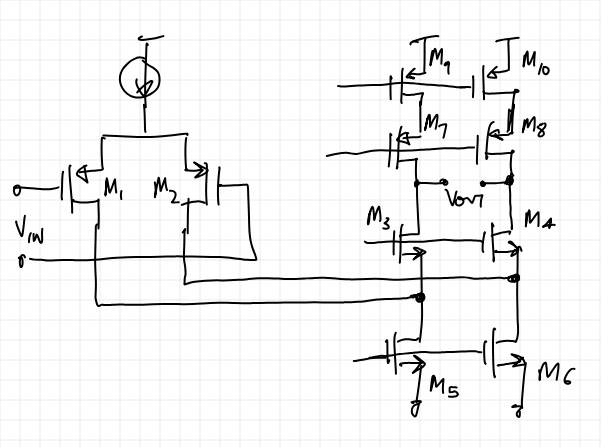
- The biasing current in either output string (current through M9/M10 see figure) should be greater than half of the tail current of the input pair (Iss). This is because in case of a large swing when 1 input pair transistor is cut off (say M2)and all the tail current comes through 1 input pair transistor (M1), if the current in the output string (ie. Through M9/M10) is less than Iss/2 then M3 will go in cut off since now M1 is supplying more current to M5 than it sinks in normal operation. M3 going in cut off will make X a high impedance node and will result in severe non linearity and gain loss at the extreme swings. If M3 does not go in cut off then X remains a low impedance node and the operation is not affected severely.
-
- The question whether we should have resistor load or active current sources as the load for the diff pair stage of a folded cascode should be given thought. The folded cascode with current sources is shown above. Folded cascode with resistor load for the diff pair is shown below:
-
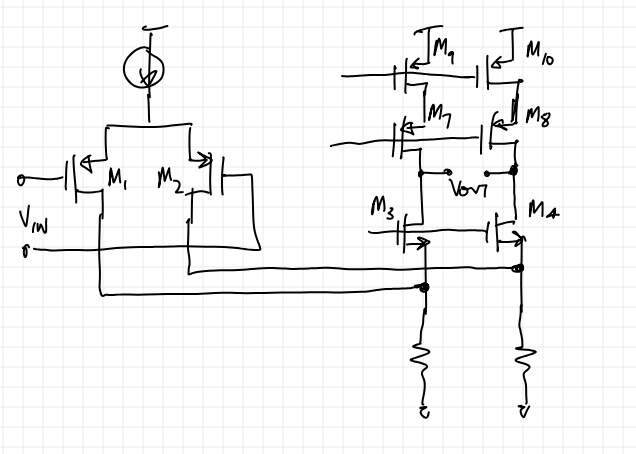
- Things to consider are:
- Resistor load provides less capacitance on the fold load at the cost of reduced gain of the diff pair stage. Even though you may thing that the gain of the diff pair with the fold node is already less because of the 1/gm impedance seen on the fold transistor (M3 and M4) sources but for the offset contribution of M3 and M4 it matters. If the we have more gain on the diff pair with its load then the delta Vt of the M3 and M4 gets divided by the gain. If we have current sources then their offset contribution generally becomes insignificant. This allows us to make these devices smaller and thus reduce the folded node capacitance and speed.
- The fold node capacitance depends on the source capacitance of M3/M4, drain capacitance of M1 and M2 and if using current sources then drain capacitance of M5 and M6. The drain capacitance of M5 and M6 can be reduced by using small cacode transistors on top of the current sinks. M3 and M4 are supposed to be strong transistors with large gm so a large W/L but making W large makes the sidewall capacitance larger.
- NOTE For the same WxL area a smaller W/L of M3/M4 would be faster for the fold node since the fold node only sees the size of W and its side wall capacitance as the loading on the fold node. The same is true for M1 and M2.
- So it can be that using current sinks with cascode may provide better speed since now you can reduce the fold transistors (M3 and M4) in WxL area significantly without affecting the offset at the same time keeping W/L large to help with the gain of the fold to provide better performance.
-
Gm Stage Design Tips
When designing a transconductance stage with a controlled and accurate transconductance follow these tips:
- Make sure you have the transconductance calculation correct. The transconductance doubles if the output is converted from differential to single ended.
- Always take into account the finite gain of source followers before the gm stage since that reduces the Gm as from what you might expect. Especially if source followers have body effect also since that reduces the source follower gain significantly.
Simulation Testbenches
Diffamp Gain and Phase plots
See Also: Differential Test Bench
Generally an opamp by itself is tested in the open loop for the Gain and Phase plots using the test setup shown in the figure:
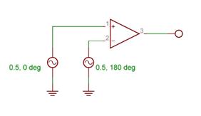
In the above case are giving a input differential voltage of 1 and a common mode of 0. So at the output we look at the Gain and Phase plots and since we assume that the worst case feedback configuration that it will be used in will be with β=1. So we aim to make the open loop gain and phase plots to have sufficient Phase Margin to be stable.
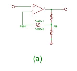
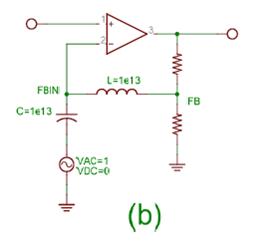
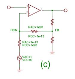
Another case is like we design an opamp to be used inside an integrated Circuit as a sub block, in that case we already know what is going to be the feedback configuration of the opamp so in this case we must include the feedback configuration and then find the gain and phase plots of the loop as a whole. So what should be ideally done is to run a transient simulation and store the node voltages in a file. Now break the feedback loop and place AC source at the end of the loop which goes into the opamp, and then plot the gain and phase plots at the other end of the loop. This can be done using the following circuit configurations (Each takes the example of a simple resistive feedback):
Circuit (a) can be used also to do the transient simulation since the AC voltage source won’t affect it. But when the AC simulation is done then the Magnitude plot should be plotted for Vdb(FB) – Vdb(FBIN) and the phase plots should also be plotted for FB-FBIN, so it is sort of inconvenient. Also see the Feedback Loop gain calculation analysis, this will not give the total result if the input impedance is not infinite, we need to calculate it using a test current source also and then calculate the actual loop gain from the combination of the results. So the point to break the loop is important if accurate results are needed by just 1 analysis.
Circuit (b) shows another way to do it but this circuit cannot be used in the transient simulation since inductors and capacitors make the transient simulation slower. So it will be inconvenient to use it also.
Circuit (c) shows a way to do this and this circuit can be easily used in the transient and AC Simulations both. The drawback here is that it isolates node FB by the loading of node FBIN during the AC analysis so if FBIN has some loading (like finite input impedance of the amplifier) it will not come in the analysis and give an inaccurate loop gain, so the point to break the loop is important.
NOTE: One thing that I found out painfully is that APS messes up this simulation. If you put resistor values different for AC and DC simulations in the resistor be sure to run the simulation using Spectre and not APS if using Cadence.
NOTE:
- In each of the cases above we are not doing a pure Diffamp simulation since in each case the differential input voltage is -1 but we also have a common mode AC voltage input at the inputs since we are only applying the AC voltage at only 1 terminal so the common mode input is (V+-V-)/2 = -0.5. This can be solved by having a similar arrangement on the other opamp terminal.
- The phase seen at FB node will be -180 when the opamp circuitry does not add any delay to the signal. It just adds the negation which gives the -180 phase, as the opamp circuitry adds delay the phase starts reducing more and the phase should reach -360, which would be the unstability condition in this case since it will reinforce the signal. This is different than the normal Diffamp simulation since in that we are having the reference input as the input to the +ve terminal and test the phase at the output considering it will be fed to the –ve terminal, thus a phase lag of 180 deg wrt +ve terminal when applied to the negative terminal will reinforce the input signal and hence cause instability. In this case we are just looking at 1 node, so the numbers are changing.
Transconductor Testbenches
Gm vs Input common mode voltage
To get the Gm vs input common mode voltage plot:- DC short both transconductor inputs but have a AC input of 1V.
- At the output put a DC source of the proper output common mode voltage.
- Do the AC simulation while sweeping the input DC voltage and plotting the output DC source current. This plot is the Gm vs input common mode plot.
- From this plot measure the input common mode range for the desired Gm band.
Gm vs Large signal input voltage sweep
To get the Gm vs input voltage do the following:- Either sweep both inputs in a complementary way or bias 1 input at a reference and sweep the other from a low voltage to a high voltage which would cover the full input dynamic range (that it is designed for). Choose the right one according to application in circuit.
- Plot the output current out of the transconductor.
- Gm curve is obtained by dividing the derivative of the output current by the derivative of the input voltage: dIout/dt by d(V+ - V-)/dt. From this curve the input dynamic range can be measured for the allowed Gm degradation band.
- Also from this simulation measure the Maximum source and sink currents when the input voltage is at the extremes.
Maximum Output Swing/Dynamic Range
To get the Output Dynamic Range do the following:- Either put the inputs in 1 way extreme and with the output current maximum in 1 direction sweep the output voltage to the point the output current degrades by a certain amount. This output voltage is the limit.
- Do the above for the other extreme.
References
- Simulation Guidelines
- Thermal Shutdown Comparator
- Refer Opamps for notes an theory.
