Think of PCB as a component of the Design
Current Capacity
Found this table on PCB current capacity in one of TIs Application NotesThis presentation gives these rough numbers:
| Trace Width | Current |
| 0.010" | 0.3 Amps |
| 0.015" | 0.4 Amps |
| 0.020" | 0.7 Amps |
| 0.025" | 1.0 Amps |
| 0.050" | 2.0 Amps |
| 0.100" | 4.0 Amps |
| 0.150" | 6.0 Amps |
Parasitics
Traces
- Refer Chapter 17 Section 17.4.4 from Opamps for Everyone
- Keep traces as short as possible. Also use narrow traces if long traces are required – aim is to keep the parasitic capacitance minimum.
- Keep a gap of around 3 times the signal trace width between traces to minimize coupling between traces, or the minimum width between pins of an IC.
- Keep some rule of thumb numbers handy to calculate the parasitic inductance and capacitance of traces, and thus impedances at the frequency of operation.
- The most common glass-epoxy PCB material (FR4) has a dielectric constant of about 4.3. To make a trace with a characteristic impedance of 100 Ohm, use a trace thickness of about 0.4 times the thickness of the board with a ground plane on the opposite side. For a 50Ohm trace make it 2 times the thickness.
- Keep analog signal traces away from digital traces, there should be no overlapping anywhere.
- In the end round of trace corners as the finishing touch to keep uniform trace width so that the transmission line characteristics are not disturbed and there are minimum reflections.
- Make sure the traces to the inverting inputs of Opamps are small. Also they do not parallel with the trace to the non inverting terminal for a significant length. Aim is to make the capacitance between the 2 terminals minimum to prevent pole from becoming low frequency.
Power and Grounding
- In 4 layer boards, it is better to put the power and ground planes internal to take advantage of the distributed capacitance between them. Putting them external so that signals can be routed between then to prevent EMI interference does not give many benefits since the leads of components mounted on the board would destroy all the benefits by acting as the antennas. Another advantage is that signal routes as available for probing. In more than 4 layers high speed signals can be shielded in between.
- Use separate power and grounding planes for Analog and Digital Circuitry
- Do not overlap these planes at any place on the board, place analog power coincident with analog ground, and digital power coincident with digital ground.
- Have a single low impedance connection point to the ground and power planes, if they are ultimately the same net. That single point should be preferably closest to the supply or can be the chassis.
System
- Have completely different analog and digital sections on the board so that the signals are separated.
Analog Circuitry
- Keep analog circuitry close to the power connector of the board to prevent noise coupling on the power lines.
- Ultralow-power oscillators Low Frequency mode should be guarded from noise coupling from other sources. The crystal should be placed as close as possible to the clock generator chip with the crystal housing grounded and the crystal traces guarded with ground traces.
Block Specific
Switching Regulators
Discussion
The most important things in the switching regulator board layout are:- The Power Path - the path which delivers the power. This is critical since it determines your efficiency and carries the power and switches at high speeds causing ringing and other effects.
- Switching paths - any switching current path - need to minimize inductances.
Design Points
Component Placement
- Check the current loops for each switch position and minimize those loops (Make those loops tighter). Examples:
- For a high side switch on in a buck the current path is from the input capacitor -> HS switch -> Inductor -> Output Capacitor -> Input Capacitor
- For a low side switch on in a buck the current path is from the LS Switch -> Inductor -> Output capacitor -> LS Switch
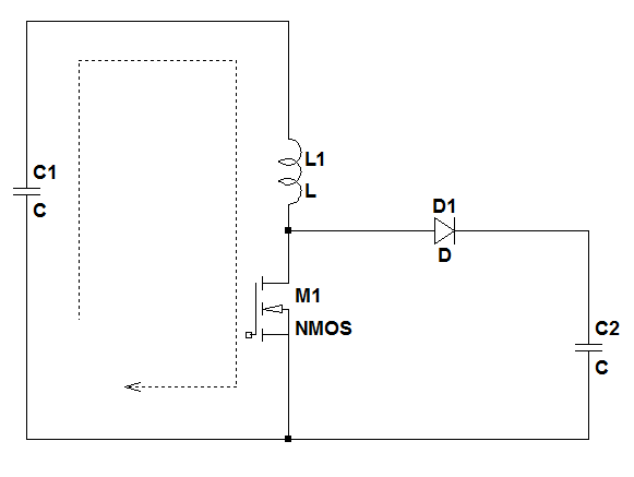
- For Boost this is the first loop:
- And this is the second loop:

LX node
- Capacitance of LX node causes LX ringing so minimize the LX flood area and make sure it does not overlap and GND or VIN plane to minimize capacitance. See LX Ringing on Switching Regulators
- Inductances in the HS/LS fet leads cause ringing when the FET turns ON so minimize that by making the shortest path without any vias. This is important only upto the LX node. From the LX node to the inductor you already have an inductor there so inductance on that path is acceptable.
Feedback
- Feedback resistor divider and feedback line is important since it goes to a high impedance point and can pick up noise easily so:
- Keep it far from the Inductor
- Place the sense point right at the output capacitor (which is close to the output load)so that you have minimum power ground disturbances on the feedback path
References
- General PCB Design Guidelines
- Basic Switching Regulator Layout Techniques - Very nice article from Maxim Author on EDN about Switching Regulator board layout
- PCB layout guidelines for Power Controllers - Talks about layout guidelines for switching regulators
- Grounding in High Speed Systems - Talks about Grounding of switching regulators and boards in general with noisy and quiet circuitry on board
- Layout Guidelines for Switching Power Supplies - Talks about layout guidelines for switching regulators (from TI)
References
- PCB Design Presentation - Talks about everything in PCB layout and manufacture a little bit
- PCB Design Tutorial - Talks about designing PCBs with CAD tools had has good guidelines on doing layout
- PCB Basics for beginners - Nice article talking about PCB basics