Here I discuss my analysis of the gm/Id methodology
Main Points
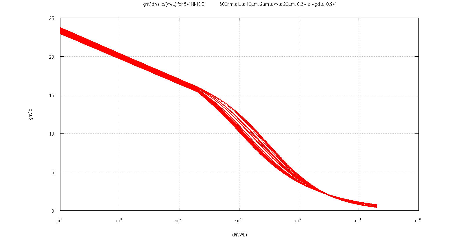
- gm/Id vs Id/(W/L) graphs for MOS devices in 1 technology intend to be constant for a particular device. This I tested in all processes I have worked on. The curve when plotted using Cadence looks like this:

- If a constant graph exists then all we need to design is just get a graph for each MOS model and a lot of information would be readily available to design and to analyze existing circuits.
- Basic approach for using the graph for design is :
- Find the gm/Id value based on the topology specification equations or choose them by choosing the area for biasing.
- Read the normalized current values Id/(W/L).
- Determine the Id and L as independent parameters from design specifications to get the size of the devices.
- For analyzing circuits this makes a great tool since now by looking at the size of the device and the current through the device you know the exact gm of the device by looking at the graph, which becomes almost as convenient as finding the gm of bipolar transistor circuits.
The gm/Id vs Id/(W/L) graph
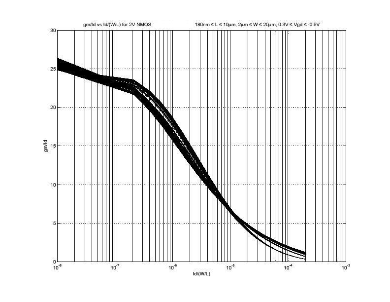
The graph below shows the graph taken from another technology for a MOS device:
As can be seen all the family of curves nearly lie at the same place. So now if we know the current we can choose an operation point and determine the right size just by looking at the graph. For example for a high gain device choosing a gm/Id of 20 and if the current is 5uA then we know the gm is 100uS and the corresponding Id/(W/L) is about 5e-7 which means that W/L = 5e-6/5e-7 = 10. Choosing an L with other constraints like matching or capacitance will give the size of the device directly!
Optimizing with Speed, Power, Gain
Speed
To optimize the efficiency with the speed of the circuit we need a parameter to characterize the speed of the device. That parameter is fT - unity gain frequency which for a MOS device is gm/(Cgs+Cgd). This is easily derived assuming the drain is grounded and the current into the gate should be the same as the current being pulled into the drain of the MOS (This doesn't seem useful from an application standpoint since the drain is grounded and the drain capacitance is ignored, also an ideal current into the gate removes the affect of series gate resistance and the drain grounded removes the affects of Cgd on the drain that is why Lee suggested unity power gain frequency parameter in his book: The Design of CMOS Radio-Frequency Integrated Circuits, Second EditionFor a square law device fT=K.gm/Id.(1/L^2)
So if you have an idea of the fT then by choosing a L you can get a gm/Id number. This means you need to select 2 of the given 3 to determine the other:
- fT
- gm/Id
- L
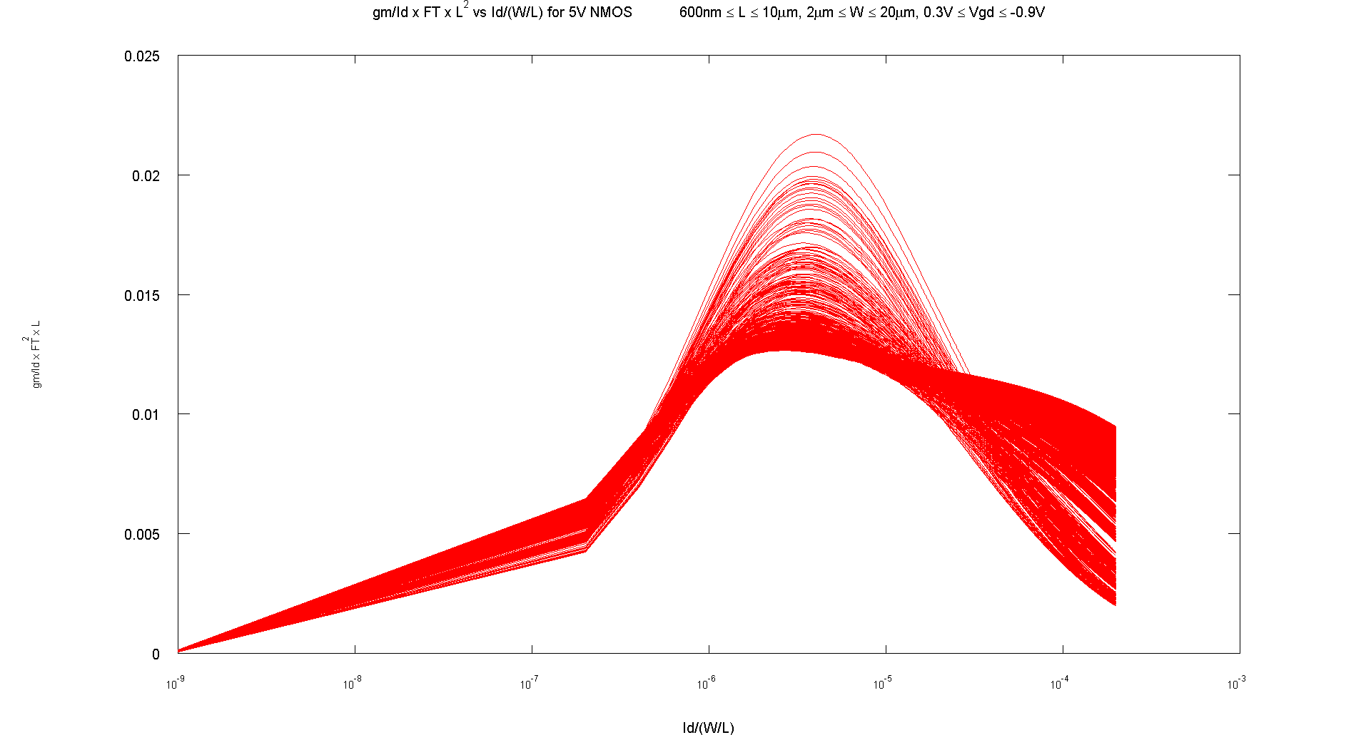
The graph below shows the gm/Id*Ft*L^2 vs Id/(W/L) graph for 5V NMOS transistors for a process:

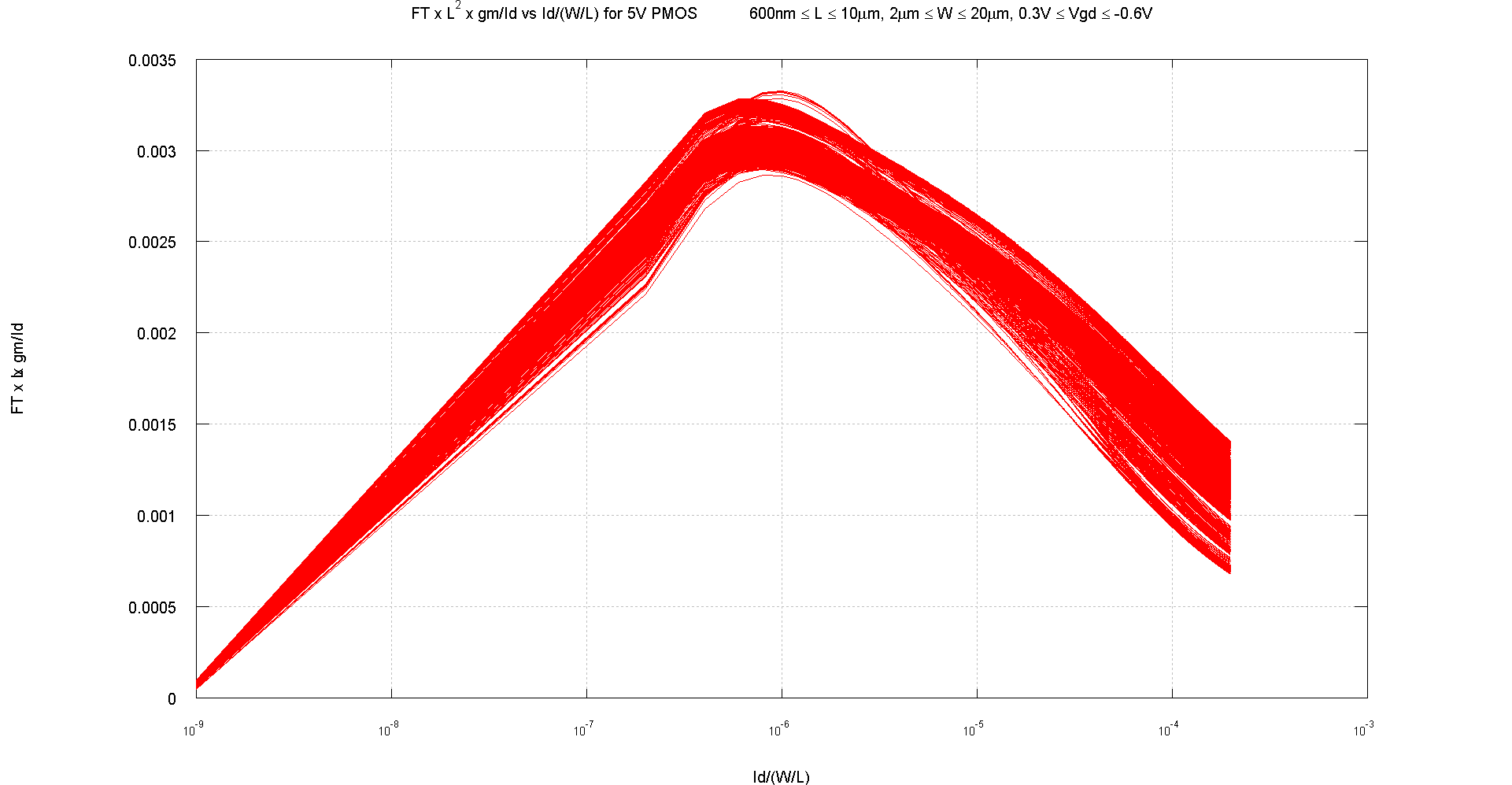
The graph below shows the gm/Id*Ft*L^2 vs Id/(W/L) graph for the 5V PMOS transistors in the same process, looks much more consistent than the NMOS transistors. It could be that the extra vgd range in 5V NMOS causes the difference:

The most interesting thing is that both graphs show a peak of this parameter. Thus there is an optimum point which maximizes efficiency and speed for a wide range of device sizes and it roughly lies at the same normalized current value. Hence it can be a useful default design point to set transistors to or to start from.
It is also useful to know the maximum speed you can get for given size and current you allow a device.
Power
Power is almost always a spec to be considered. Power directly comes into consideration in the gm/Id methodology since it is directly proportional to Id with a fixed supply which is usually the case.So usually you need to select 2 of the given 3 to determine the other:
- Transconductance
- Current
- Power